THz near-field probing adds a contactless, non-destructive localization step ahead of destructive preparation — electrically, by time-domain reflectometry with a 0.6 ps pulse launched at the device, and structurally, by near-field imaging through mold compound and polymers.
Failure analysis is a chain of expensive, destructive steps. The more precisely a fault is localized before the first cut, the less preparation, FIB time and sample material it costs — and the less likely the defect is destroyed on the way.
LIT, TDR, X-ray …
New THz TDR · THz near-field imaging
Laser, FIB, RIE, wet chemistry, milling, abrasive blasting …
SEM / EBSD, EDX, TEM, ToF-SIMS …
Image correlation, ESPI …
Steps 02–04 are where time and cost accumulate. Every gain in localization accuracy at step 01 shrinks the volume that has to be prepared.
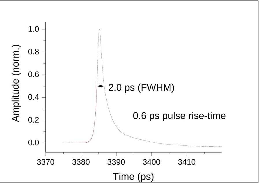
In TDR, two discontinuities can only be told apart if they are further apart than roughly vg·tr/2. Electronic TDR is limited by its microwave signal path — the THz pulse is generated and detected on the probe itself, directly at the device.
| TDR approach | Signal path to the DUT | Rise time at DUT | Rise time, linear scale |
|---|---|---|---|
| All-electronic TDR | Pulse generator, cables, microwave probe | > 10 ps | |
| Electro-optic TDR, microwave chain | On-chip photoconductive switch, waveguide transition, hollow waveguide, microprobe (< 110 GHz) | ≈ 6 ps* | |
| THz TDR microprobe | None — photoconductive switches integrated in the probe tip | 0.6 ps |
* Datasheet value of a commercial electro-optic TDR system. THz figure: probe-integrated pulse without DUT, 0.6 ps rise time, 2.0 ps FWHM (Nagel et al., Opt. Express 2011).
THz penetrates mold compound, polymers, ceramics, glass and high-resistivity silicon; metals reflect. The radiation is non-ionizing and needs no sample preparation.
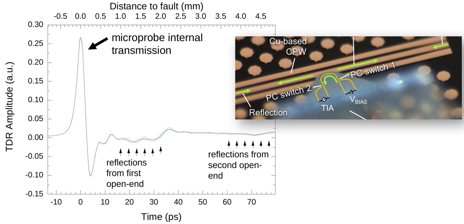
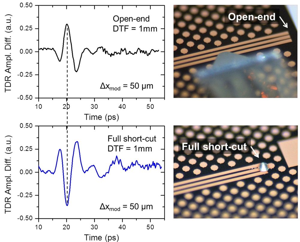
A sub-picosecond pulse is launched into the interconnect directly from the probe. Every discontinuity reflects part of it; the echoes locate and classify faults along the line — open, short or partial.
The probe is raster-scanned over the package in transmission or reflection. The result is a set of amplitude and phase maps — and in reflection, time-of-flight slices through the package depth.
An LT-GaAs photoconductive switch sits in a µm-scale electrode gap at the very tip of the probe. A femtosecond gate pulse — 780 nm, or 1550 nm-compatible versions — makes the gap conductive for less than a picosecond.
The local near field of the device biases the gap. There is no galvanic contact and no RF interconnect; the stand-off ranges from a few µm to about 100 µm. The unscreened, non-resonant tip keeps the field perturbation low.
The gate-synchronous photocurrent is proportional to the field. A delay scan reconstructs the full waveform. Probe orientation selects Ex, Ey or Ez; transceiver probes carry emitter and detector on one tip.
Test structure: a Cu-based coplanar waveguide on a silicon chip. The THz TDR microprobe carries two photoconductive switches — one launches the pulse into the line, the other detects what comes back.
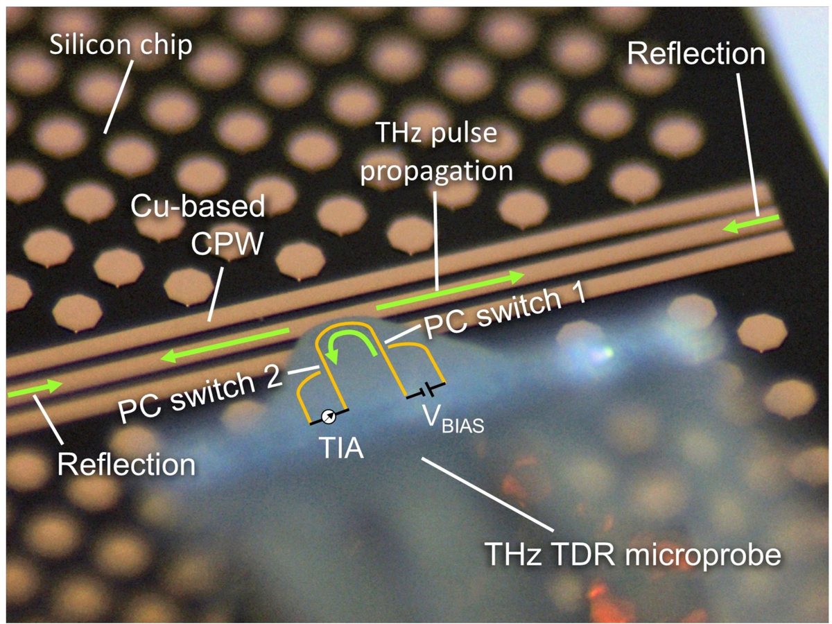
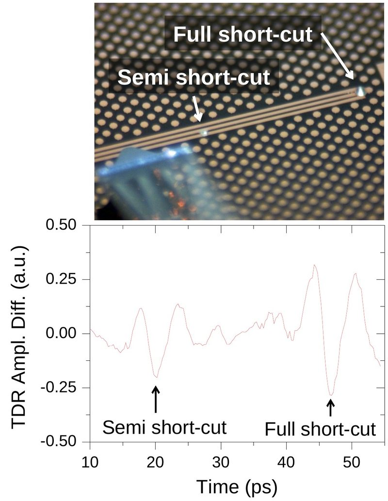
Artificial defects on test structures. The sign of the echo gives the defect type directly; its delay gives the distance to fault (DTF).
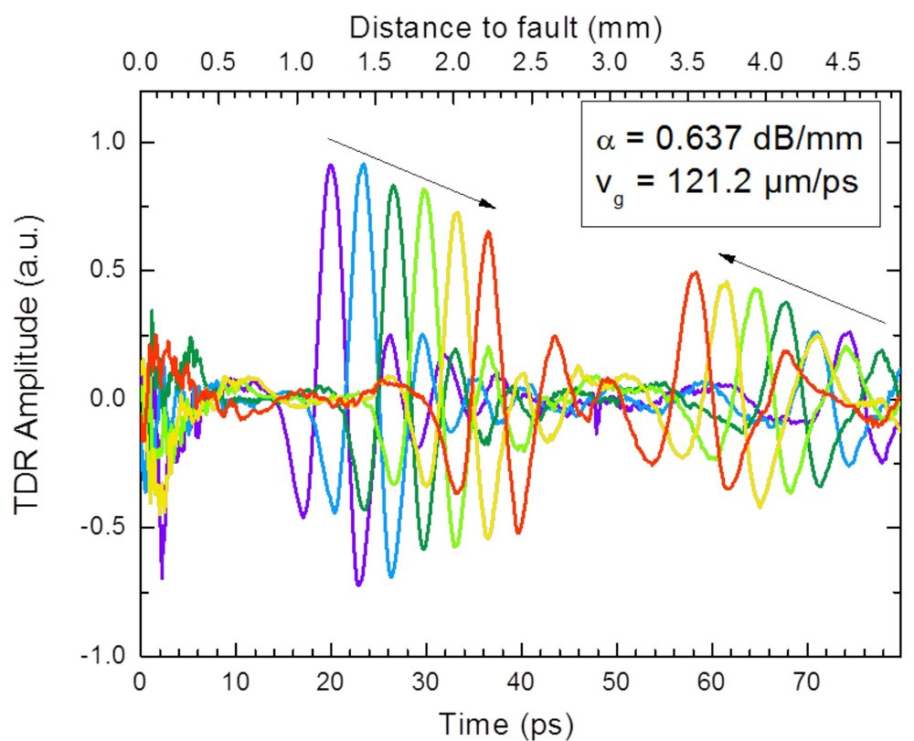
Measured on the Cu-CPW; converts echo delay to distance.
Extracted from the echo decay along the line.
Open, short and semi-short located at this distance.
Echoes detected up to this distance on the lossy on-chip line.
Numbers derived from the measured rise time and the group velocity on the Cu-CPW test line. Absolute sensitivity depends on coupling and device, and has to be determined on your structures.
Near-field imaging in transmission gives fast lateral contrast; reflection adds depth. Both work contactless on assembled parts.
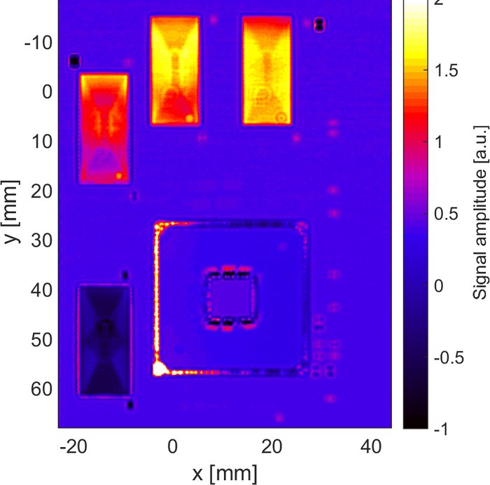
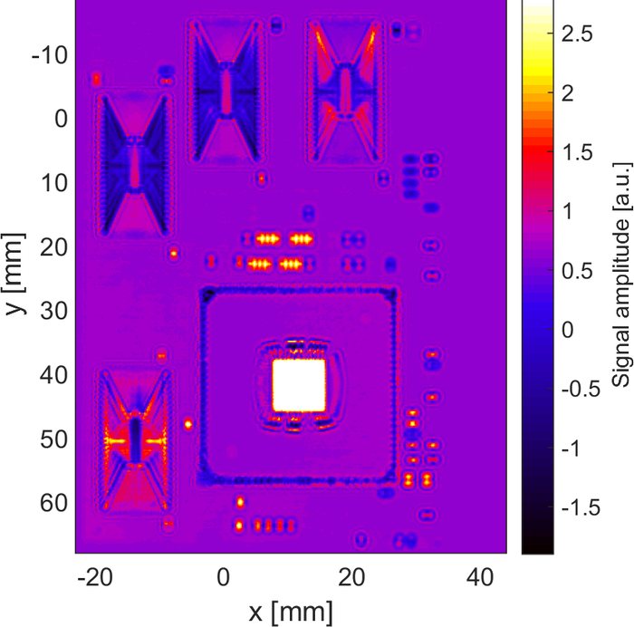
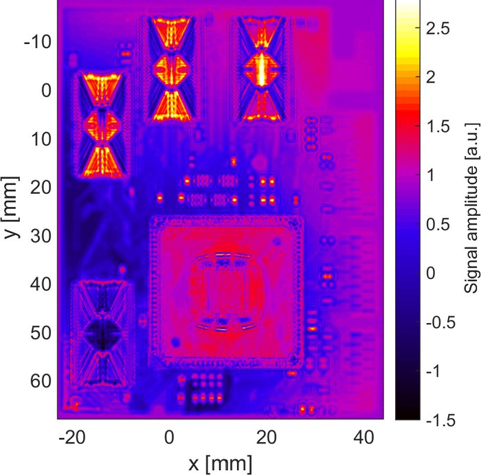
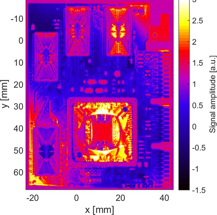
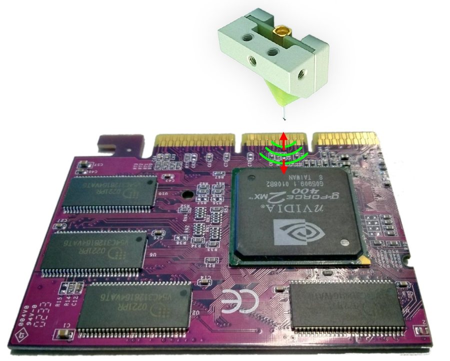
A transceiver probe is raster-scanned above a graphics-card module. Different time windows of the reflected transient address different depths — package surface, internal lead and bond structures, die area.


One scan, four time windows of the reflected transient. Field of view about 65 × 85 mm². Demonstration sample: a commercial graphics card.
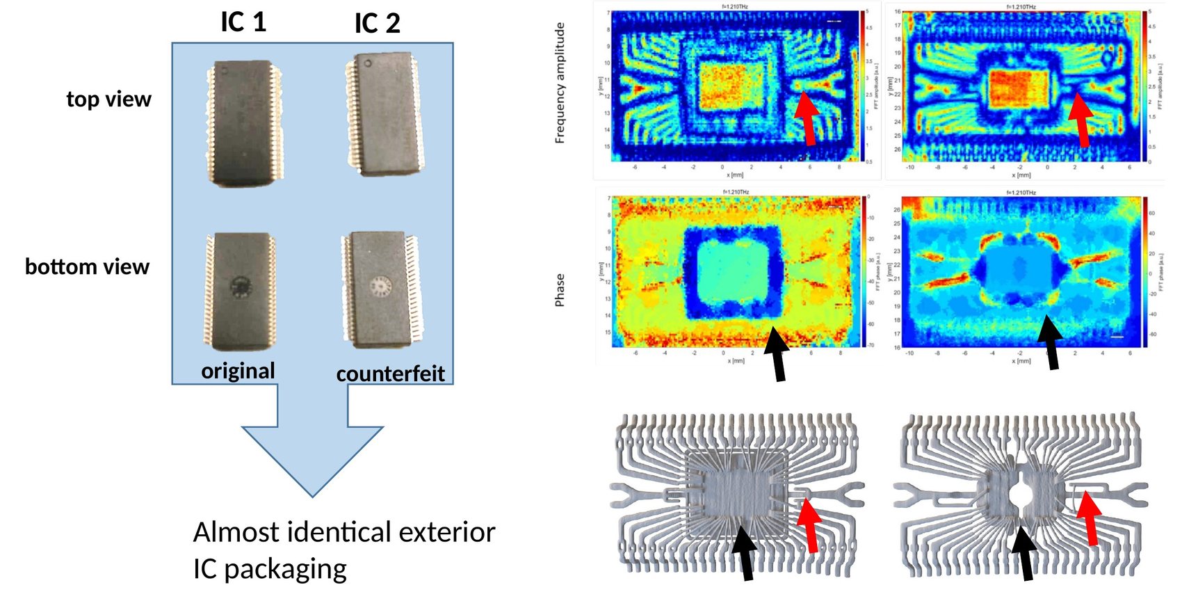
An original and a counterfeit IC, externally indistinguishable. Amplitude and phase maps at 1.2 THz resolve clear deviations in the die area and the lead structure — consistent with the X-ray reference.
Sparse deconvolution turns the reflection transients into depth-resolved reflector maps: die position, pads and bond wires. The die of the counterfeit sits at a different depth — information not accessible in transmission.
Wafer-level sheet-resistance mapping of conductive layers →
Probe, scanner, analysis — configured for transmission, reflection or TDR.
Whether THz fits your failure-analysis flow depends on the package, the line and the defect. The fastest way to find out is a measurement.
We measure your device or test vehicle in Aachen, deliver maps, traces and raw waveforms, and tell you what the data does and does not support.
For new applications: mutual NDA, your use cases and test structures, a feasibility study at Protemics — and a clear statement of where the method ends.