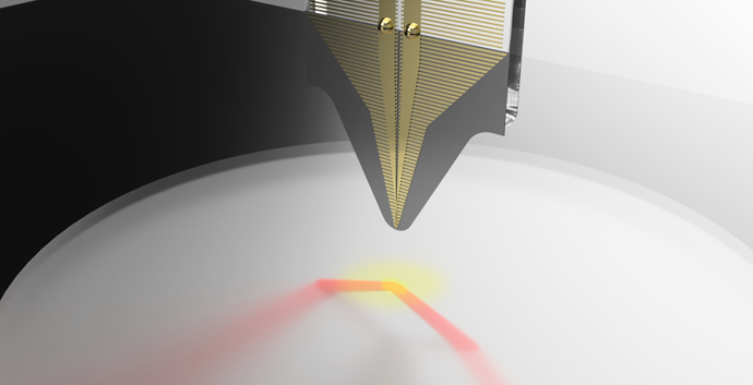
One of the most important applications of the TeraSpike probe lies in the field of wafer analysis. So far, it has been mainly used to probe wafer material properties such as sheet resistance or charge carrier mobility under normal ambient conditions. Now a team of researchers from the Dutch institutes DIFFER and Eindhoven University of Technology succeeded in demonstrating the use of the TeraSpike near-field probe for measurements of wafer conductivity under short pulse optical excitation.
The team led by Prof. Gómez Rivas and Dr. Halpin showed that it is possible to map relaxation properties of optically excited charge carriers with a spatial resolution 10-times smaller than the applied THz wavelength and - thanks to the sub-ps time-resolution of the TeraSpike - from ultra-fast to ultra-slow trapping processes. In their recent article in Optics Express they describe the technical details of this approach.