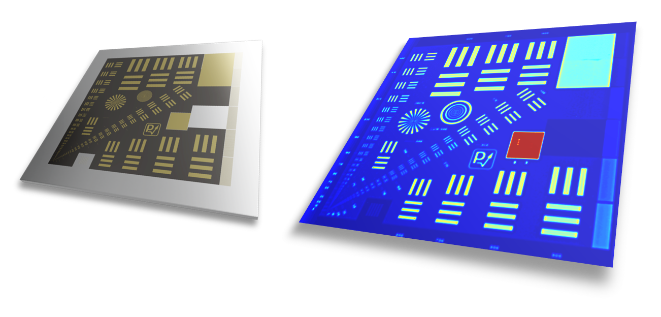
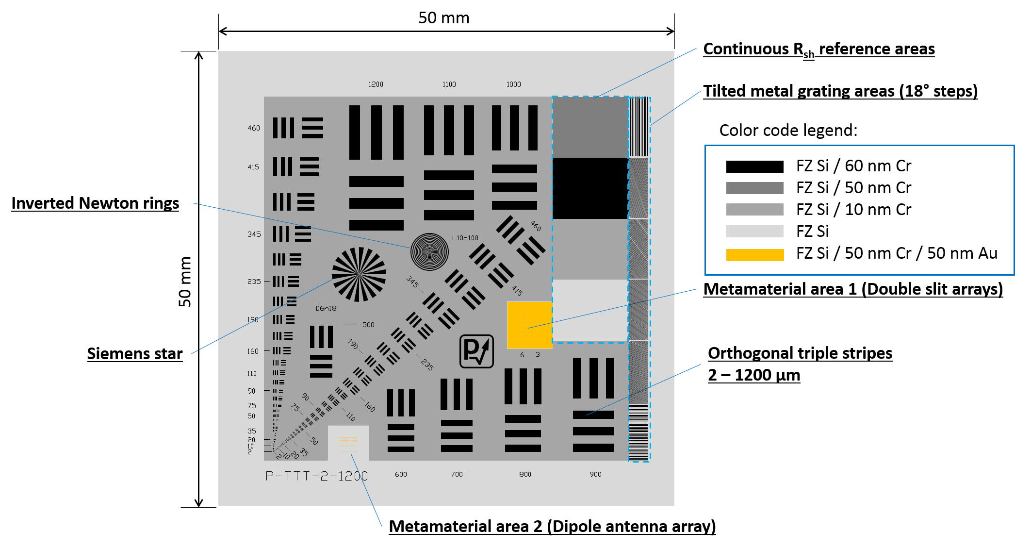
Target design model: P-TTT-2-1200
The test target P-TTT-2-1200 has been specially developed for the characterization of Terahertz imaging systems. Featuring structures and areas from 2 µm up to 8 mm of lateral size it is suited for standard diffraction-limited systems as well as near-field imaging systems with sub-wavelength resolution.
The test target is based on high-resistivity silicon and contains conductor areas with three different transmission strengths beside uncoated substrate areas with maximum transmission. The featured structures include classic resolution test structures such as orthogonal pairs of three stripe structures, a Siemens star and concentric rings. These typical structures are accompanied by further structures specially useful for near-field imaging purposes such as metamaterial structures generating local field confinement. Additionally, areas helpful as references for sheet resistance imaging and wafer scanning applications are also listed.
Specifications:
P-TTT-2-1200 |
Value |
|
Substrate material |
High-resistivity FZ silicon, 2-side polished |
|
Substrate Resistivity |
> 10 kOhm cm |
| Target overall size | 2" x 2" (50 mm x 50 mm) |
|
Substrate thickness |
525 µm |
|
Coating materials |
Cr, Au |
|
Coating thickness |
Cr: 10 nm, 50 nm and 60 nm (in semi-transparent areas) Au: 50 nm (opaque) |
|
Orthogonal pairs of three stripe structures |
2 – 1200 µm wide lines & spaces 45° rotated for 2 - 460 µm wide line & spaces |
| Siemens star |
6 mm outer diameter, 18 elements |
| Inverted Newton rings |
5.6 mm outer diameter Ring widths from 10 – 500 µm in increasing steps |
| Continuous Rsh Reference areas |
Four areas, each 6.7 mm x 8.3 mm |
| Tilted metal grating areas |
Six areas, each 2 mm x 6.7 mm Tilting angles: 0°, 18°, 36°, 54°, 72°, 90° |
|
Bow-tie array metamaterial |
300 µm length, 5µm gap |
|
Asymmetric double slit array metamaterial |
3 µm and 6 µm slit width and spaces |